|
Click here to resend forum activation email
Lost your password, Request it here
Future MRT MAP has MOVED here. Click here.
SHARE
AMD G34 Socket: "Magny-Cours" 12-core Processor Unified Discussion Thread General Mainboards/CPU/Chipsets/OC-MOD

25-08-2009, 12:28 PM
|
 |
Gold Member
|
|
Join Date: Oct 2001
Location: Philippines/Tokyo
Posts: 7,688
Potenza rep: 30
|
|
 AMD G34 Socket: "Magny-Cours" 12-core Processor Unified Discussion Thread
Quote:
AMD FINALLY STARTED to publicly talk about Magny-Cours and socket G34 during the Hot Chips 21 conference. The socket has a lot of complexities, so for now, we will only take a look at the interconnects, both on chip and off.
Magny-Cours is the CPU itself, a 12-core MCM that consists of two Istanbul 6-core CPUs. Each core has 512MB of L2 cache and 12MB of L3 half of which is on each die. The package also has 4 HT links and 4 channels of DDR3/1333. Clock speeds were not revealed, but the hint was about a 25% downclocking compared to Istanbul.
|
 Magny-Cours die (i.e. Istanbul MCM)
Quote:
...In a four socket system using the 'old way' AMD did things, IE a square, two of these three (HT) links were used to connect the chips to the two neighbors. A chip in the top left would be connected to the one on the right, and the one below, but not the socket diagonally across. The third was not used.
Diagonal connections could be done, but rarely if ever actually was done. The third ccHT connection was used to connect two 4-way squares to make an 8-way system. While this was a good thing for packing in more CPUs into a box, it was hobbled by the latency caused by multiple hops across HT links. CPU 0 loading from CPU 7's memory might need 4 hops to get to the data and four hops to get back. Add in cache coherency, and you had those hops taking the whole system to it's knees.
The way around this is to directly connect each socket to every other one in the system. On a 2 socket box, that is easy, you just connect point A to point B. On a four socket, you make a square with an X in the middle, exactly what AMD traded off to allow for 8 sockets on socket F and before.
With the new socket G34, AMD did just that. (An) 8-bit ccHT link is basically a diagonal link, the X in the square. If there was only one die in each socket, that would work wonderfully, problem solved! Unfortunately, G34 has two dies per socket, and they are connected to the two dies in the other socket using one of those 8-bit links per die.
On a two socket system, the links directly between the dies are 16-bit and the ones going diagonally are 8-bit. Since there are two full ccHT links per die, four per socket to connect everything on a four socket system. To connect between sockets, you don't need the full bandwidth that a 16-bit HT links brings.
In the end, each socket is connected to every other socket directly, but every die only connected to every other die on a two socket system. The worst case in G34 is to have any die 2 hops away from any other die. It all looks like this.
|
 Socket diagrams for two and four sockets
Quote:
If you think this looks like a mess, then send flowers to the AMD engineers who had to write the routing algorithms to make it all work, and work perfectly. On a more theoretical level, the 2 way G34 is the same as the older socket F 4 way with a cross connect. The G34 4 way is like the two way, but extruded into the Z-plane.
The scheme that AMD uses for connections on a four socket system requires 3 8-bit lanes per die, 6 8-bit lanes or 3 16-bit lanes per socket. Adding a fourth link would take die space, a lot of complexity to the routing, and many more pins on the package. G34 already has 1944 pins, the most we are aware of in large scale production, and adding to that for minimal benefit is not a good idea.
To fully connect this 4 socket G34, you would need that fourth 16-bit HT link. P1 needs to connect to P2 and P7, and the cost/performance tradeoff wasn't enough justify another link. Maybe in socket G44. In any case, two hops is a lot better than the four it used to take.
AMD is quoting the average number of hops used to get to memory, diameter in AMD speak, is .75 for a 2 socket system, 1.25 in a 4 socket. In order to alleviate the problem of cache snoop traffic, AMD put in something called a snoop filter, termed HT assist in AMD speak. It is more complex when you combine it with the G34 topologies...
That is not to say that functionality drops off. The metrics AMD used to demonstrate this is DRAM bandwidth and Xfire (Crossfire, but not that ATI Crossfire) bandwidth. DRAM bandwidth is just the aggregate memory bandwidth of the system. Xfire bandwidth is how much memory is available when each core is reading from all the other cores in a round-robin fashion.
2 socket G34 systems have a DRAM bandwidth of 85.6GBps and a Xfire bandwidth of 71.7GBps. On a four socket system, those numbers double to 170.4GBps and 143.4GBps, almost exactly double. This makes sense for DRAM, but to do it on the Xfire side is a lot more impressive. It looks like the interconnects did what they were supposed to do, and adding a fourth link would not be worth the cost.
In the end, AMD fixed the two biggest problems with multiple sockets, latency. Part of that was the probe filter in Istanbul, but a much more important step was the new interconnect scheme. It isn't fully interconnected, but socket G34 is very close. For what is effectively an 8 socket system, packaged into 4 MCMs, AMD seems to have done a very good job.
|
http://www.semiaccurate.com/2009/08/...ts-socket-g34/
Jeez, I can't wait to run several dozen VM's on these babies... |
25-08-2009, 04:10 PM
|
|
Bronze Member
|
|
Join Date: Sep 2006
Location: Egypt
Posts: 836
Potenza rep: 18
|
|
wow , will there be available software to match such powerful processor? or it will wait years before even caught by one or 2 apps?
|
26-08-2009, 09:33 AM
|
|
Gold Member
|
|
Join Date: Oct 2001
Location: Philippines/Tokyo
Posts: 7,688
Potenza rep: 30
|
|

Intel Details Nehalem-EX ("Becton"):
Quote:
...Becton, now called Nehalem EX...
...looks like a simple mashing together of two 4-core Nehalems. The specs are 8 cores, 16 threads, 4 DDR3 memory channels, 4 QPI links and 24MB of L3 cache all stuffed into a mere 2.3 billion transistors. If you take a Lynnfield i3/i5/i7, add a little more cache, and weld a second one on, it looks a lot like Becton, but that is where the similarity ends.
Nehalem is a modular architecture, and about the only thing the two chips have in common are the cores themselves. Just about everything else is different between high-end Bloomfield (i7) Nehalem and Becton. Because of the modular architecture of the base chip, this could be done without enormous amounts of pain.
|
Ring Bus Block Diagram

Quote:
The biggest difference between the two is the ring bus. At 24MB, the cache is far too big to run at an acceptable speed, and making 24MB 8-ported fast cache RAM was a basically impossible task. Instead, Intel split the cache up into eight 3MB chunks called slices, and assigned one per core. That size cache is easy enough to design, and they ended up as inclusive with 4-ports.
Eight independent caches are not all that useful compared to a single large 24MB cache, so Intel put a large, bidirectional ring bus in the middle of the cache to shuttle the data around. If any core needs a byte from any other cache, it is no more than 4 ring hops to the right cache slice.
The ring bus is actually four rings (* For the eleven kings under the sky, plus some...LOL!), with the data ring being 32 bytes wide in each direction. It looks a lot like the ring in Larrabee, but Intel has not announced the width of that part yet. That said, it is 1024 bits wide, 512b times two directions. There are eight stops on the Becton ring, and data moves across it at one stop per clock.
To pull data off the ring, each stop can only pull one request off per clock. With two rings, this could be problematic if data comes in from both directions at the same time. The data flow would have to stop or the packets would have to go around again. Neither scenario is acceptable for a chip like this.
Intel solved this by putting some smarts into the ring stops, and added polarity to the rings. Each ring stop has a given polarity, odd or even, and can only pull from the correct ring that matches that polarity. The ring changes polarity once per clock, so which stop can read from which ring on a given cycle is easy to figure out.
Since a ring stop knows which other stop it is going to talk to, what the receiver polarity is, and what the hop count is between them, the sender can figure out when to send so that the receiver can actually read it. By delaying for a maximum of one cycle, a sender can assure the receiver can read it, and the case of two packets arriving at the same time never occurs.
In the end, the ring has four times the bandwidth of a similar width unidirectional ring, half the latency, and never sends anything that the receiver can't read. The raw bandwidth available is over 250GBps, and that scales nicely with the number of stops. You could safely speculate that Eagleton will have a 375GBps ring bus if the clocks don't change much.
Moving on to QPI, there is a second controller to enable four links per socket. In addition to allowing Becton to scale to eight sockets gluelessly, the chip can do two independent transactions over QPI at the same time. There are two functional blocks to assist with this, and Intel calls them QPI Home Agents (HA).
The home agents have much deeper caches and request queues than a normal QPI controller on a Lynnfield or Bloomfield part. The HAs support 256 outstanding requests, with up to 48 from one single source. For an eight socket system, this is not just nice but somewhat mandatory for scaling.
HAs don't just track QPI requests, they can also track memory requests, and do some prefetching and write posting. On top of that, they control a lot of the cache coherency between sockets, something Intel calls a hybrid coherency protocol.
Augmenting the HAs are a QPI Caching Agent, with two per core, one per HA. The Caching Agents do what they sound like they do, cache QPI requests and data. Additionally, they can go directly to local memory, not just QPI, and send results directly to the correct core as well. QPI handling is in Becton is not just more intelligent, but also much better buffered as well.
The Nehalem family is the first modern Intel part to have memory controllers on die, so the memory controller count scales with socket count. Becton has two memory controllers per die, two channels per die, and two memory buffers per channel. With four DDR3 DIMMs per channel, that means 2 X 2 X 2 X 4, or 32 for the math adverse, per socket. On an eight socket system, that means 512 DIMMs, 4TB of memory per box. That is almost enough for running Vista at tolerable speeds.
In case you didn't notice, there was something new in the memory hierarchy, memory buffers...
...it started with FB-DIMM AMB buffers and evolved things from there. If the new buffers kept the RAS features and other similar technologies, they will be a net plus for the Nehalem EX platform.
|
8-Socket Nehalem-EX (!)

Quote:
With 4 QPI links, 8 memory channels, 8 cores, 8 cache slices, 2 memory controllers, 2 cache agents, 2 home agents and a pony, this chip is getting quite complex. The transistor count of 2.3 billion backs that up. To make it all work, the center of the chip has a block called the router. It is a crossbar switch that connects all internal and external channels, up to eight at a time.
The router is fully programmable, so what it does in Becton is not the only thing it can do. You are unlikely to see anything different in this generation of product, but it could be done if needed. Eagleton should have a few new tricks, especially when it comes to routing using external glue chips for high socket counts.
With that many available inputs and outputs, you start to understand why the focus of Becton was on the uncore, and how things get moved around the die and the system in general. Without all the effort put in, just doubling up a Bloomfield or Lynnfield wouldn't scale at all, much less to the 2,000-plus cores Intel is claiming Becton will hit.
|
http://www.semiaccurate.com/2009/08/...cores-and-all/
Should make for a fairly decent torrent rig...LOL!
|
01-09-2009, 10:06 AM
|
|
Gold Member
|
|
Join Date: Oct 2001
Location: Philippines/Tokyo
Posts: 7,688
Potenza rep: 30
|
|
Magny Cours is 8 and 12 cores:
Quote:
Q1 2010 launch
AMD has confirmed...that its plan to reveal next generation Opterons known as G34 is on schedule for Q1 2010...Now we know that AMD aims for Q1.
AMD has just launched new energy efficient six-core Istanbul with an ACP of 40W (TDP 60W) and hopes to compete better with Intel’s six-core Dunnington.
AMD went one step further confirming that this Magny Cours CPU comes in two variants, first with eight cores and second with twelve cores. AMD will official band them as Opteron 6000 series and it should operate under a similar power envelope as the current highest end Opteron CPUs.
|
http://www.fudzilla.com/content/view/15279/1/
vVo07!, VMWare Vsphere will love these puppies...
|
03-09-2009, 09:50 AM
|
|
Gold Member
|
|
Join Date: Oct 2001
Location: Philippines/Tokyo
Posts: 7,688
Potenza rep: 30
|
|
"Magny-Cours" - Some Design Compromises were needed...:
Quote:
...Due in 2010 on AMD's 45nm SOI process, Magny-Cours uses the same basic core microarchitecture as the current Shanghai quad-core server processor, so if there's any improvement in per-thread performance it will have to come from better system design.
The basic idea behind Magny-Cours is simple: take two six-core Istanbul processors, downclock them a bit to reduce power, and squeeze them into a multichip module (MCM) so that they can fit into a single socket. By using an MCM, AMD will be able to fit 12 cores into the same thermal and power envelope as Istanbul.
Making this work requires a few tradeoffs, and one of them is the MCM itself. AMD had previously ridiculed Intel's use of an MCM...(b)ut with Nehalem cleaning up in per-core absolute performance, AMD is having to hustle to maintain a credible server presence, and part of that hustle is adopting the MCM strategy that it had formerly ridiculed.
For system architecture reasons, AMD's MCM picture is a little more complex than was Intel's, because each Istanbul chip has its own on-die dual-channel DDR3 memory controller, along with four HyperTransport links. Obviously, you can't push each chip's full interconnect bandwidth through a single socket, so AMD had to cut out some links.
The company's MCM 2.0 design has four total HT ports (two per chip) and four DDR3 memory ports (two per chip) on each MCM. For each individual chip, one of the links is x16 and another is x8. The two chips are connected inside the module by a x16 HT link.
Even with four HT links and four memory channels to keep the MCM fed, 12 cores is still a lot to pack into a single socket, and bandwidth starvation is a concern. To help alleviate the bandwidth pressure AMD's Istanbul made a very smart tradeoff in the form of HT Assist, and this tradeoff is carried over to Magny-Cours, where it's even more necessary.
One of the big challenges in multiprocessor system design is keeping the various processors' caches in sync with one another; solutions to this problem all involve some amount of communication among the processors, and this "snoop" traffic eats up valuable bus bandwidth. The solution that AMD has adopted with Istanbul and Magny-Cours involves setting aside 1MB of each chip's 6MB cache to store a directory of the contents of the other chips' caches, so that by consulting this local directory each chip can avoid broadcasting a significant number of traffic-increasing snoop requests to the other chips.
The reason HT Assist works is that die area is relatively cheap compared to bus and socket bandwidth, so any trick that lets you trade some on-die transistors for a boost in real-world bus bandwidth is a win. This is in fact the basic idea behind caches of all kinds, and HT Assist's directory is really just another type of cache. Per-socket bandwidth will become increasingly precious as the number of cores in each socket goes up...
After Magny-Cours, AMD intends to keep upping the per-socket core count while maintaining backwards compatibility with Magny-Cours' and Istanbul's socket, power, and thermals.
|
http://arstechnica.com/hardware/news...server-cpu.ars
HTH.
|
14-09-2009, 08:54 PM
|
|
Gold Member
|
|
Join Date: Oct 2001
Location: Philippines/Tokyo
Posts: 7,688
Potenza rep: 30
|
|
Last edited by Woody : 14-09-2009 at 09:07 PM.
Reason: * typo;
|
18-09-2009, 10:13 AM
|
|
Gold Member
|
|
Join Date: Oct 2001
Location: Philippines/Tokyo
Posts: 7,688
Potenza rep: 30
|
|
Coming (Soon) to a Desktop Near You...:

 http://www.xtremesystems.org/forums/...d.php?t=234105
Quote:
|
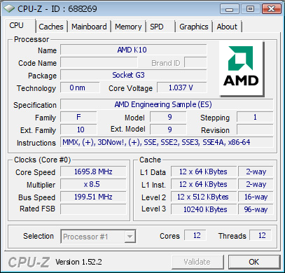
The cooling was pretty weak(standard opty coolers) and volts were very low...
|
Holy hot shorts Batman!...
|
19-09-2009, 11:11 PM
|
|
Gold Member
|
|
Join Date: Oct 2001
Location: Philippines/Tokyo
Posts: 7,688
Potenza rep: 30
|
|
Magny-Cours is "Lisbon" x2:
Quote:
|
...AMD is using lower power Lisbon cores to make Magny Cours 12-core non native core work. Magny Cours is a server CPU and we don’t expect desktop version of 12 core CPU anytime soon.
|
So just what is "Lisbon"?
Quote:
...Now, today, we introduce new Six-Core AMD Opteron EE processors that have the same 40W ACP. Again, the simple math says 40W ACP / 6 cores = ~6.67W per core. Does anyone remember the world before AMD introduced the first AMD Opteron processor?
Server state-of-the-art, B.O. (Before AMD Opteron), was Prestonia, a single core processor with configurations of up to 58W max TDP just one core! A mere six years later, the new Six-Core AMD Opteron EE processors have six times the number of cores and dramatically lower power per core.
We really have come a long way, with as much as 58 watts of power for a single core (2.0GHz), to today’s new standard of single digit ACP per core. With the shorter pipelines and better efficiency of today’s AMD Opteron processors, I am guessing that a single 2GHz Opteron core is going to be much more efficient than the legacy NetBurst cores in Prestonia, and the fact that the power is so much lower means that we are really heading in the right direction.
Next year, we plan to introduce the “San Marino” platform, featuring our “Lisbon” (C32) processor. We expect to have a platform that is specifically tuned to the needs of these very low power environments. It may not be a stretch to say that with next year’s optimized platforms, we may be able to provide even lower total power consumption than we see today with these AMD Opteron EE processor-based platforms.
Now, the question is “how low can you go?” Well, only the future will know. Well, that and our design engineers.
|
http://blogs.amd.com/work/tag/lisbon/
|
22-09-2009, 09:15 AM
|
|
Gold Member
|
|
Join Date: Oct 2001
Location: Philippines/Tokyo
Posts: 7,688
Potenza rep: 30
|
|
AMD [finally] launches own server platform: Meet Fiorano, Kroner
Quote:
AMD finally launched its own SR5600 series of chipsets, formerly known under codename Fiorano. What makes this launch probably as the most important one for AMD to date was the fact that this is the first server/workstation chipset for AMD. Given that AMD openly told us that they're gunning for servers only and they don't have the guts to challenge Intel on Workstation field, we'll consider this as server chipset alone.
Fiorano platform is consisted out of AMD SR5670 and SR5690 Northbridge and SP5100 Southbridge chips with built-in support for AMD Vi, hardware virtualization acceleration [IOMMU - Virtualization I/O]. Northbridge comes with no less than 42 PCIe lanes and 11 controllers [you've guessed it right, 790FX was the base for this chip], while Southbridge comes with all the standard features expected from a server chipset. The interesting bit is that AMD connected ATI ES-1000 GPU to Southbridge rather than Northbridge, using a PCIe x4 connection. Then again, for servers you really don't need more.
|

AMD Diagram SNAFU - RDDR-3 support doesn't come with either Istanbul nor Shanghai, rather in 2010
Quote:
Dual Socket [2S] platform comes with one SR5600 series chip offering afore mentioned 42 PCIe lanes, while Quad Socket [4S] comes with either one or two SR5600 chipsets, offering up to 84 PCIe Gen2 lanes. At launch, AMD is offering this platform with faithful Socket 1207, supporting dual-core Santa Rosa, quad-core Barcelona & Shanghai and sexa-core Istanbul processors.
Additionally to SR5690, AMD is also introducing lower-tiered Northbridge chips: SR5670 and SR5650. You can probably see the similarities between chipsets and ATI Radeon naming convention - xx90 is the fully featured chip, with xx70 and xx50 losing features to get the price or the power envelope lower.
As you can see in the picture above, AMD made one mistake - Socket F platform does not support RDDR-3. In early 2010, AMD will introduce two new RDDR3-supporting sockets for their server platform, Socket C32 and G34. As expected, Socket C32 will succeed current Socket F [1207] for the regular server, while Socket G34 will introduce dual die [MCM, Multi-Chip Module] design with two four- [San Paulo] or six-core processors [Magny-Cours]. In a way, the platform AMD is launching today is nothing more than four to six months time to optimize the chipset inside the OEM systems and motherboards to be ready for C32/G34 rollout.
Beside the layout typo, we do feel that AMD made two significant "FAIL" in this launch, with first one being partner [and user] friendliness. The official name for what was known as the Fiorano platform is "Six Core AMD Opteron processor with AMD Chipset platform" - think of it what you may, but we feel that Opteron PR and marketing division should get a lesson from ATI folk on naming conventions. AMD's "Six Core AMD Opteron processor with AMD Chipset platform" versus Intel's "Nehalem-EP" and "Nehalem-EX" platforms just doesn't cut it. Instead, AMD partners are simply continuing to use "Fiorano", "Maranello" and so on. Then again, codenames in relation to Ferrari locations and Formula One racetracks just sound much better than Texan-crew could ever come up with, as a dire consequence of key AMD personnel departing AMD in the past three years [including ones that came up with Ferrari/F1 codenames].
Beside "Six Core AMD Opteron processor with AMD Chipset platform" [ex-Fiorano], AMD also launched Kroner server specification. In a nutshell, AMD Kroner is a new motherboard design that enables OEMs to put two dual-socket servers into a single 1U or 2U chassis, i.e. even four dual-socket servers into a 3U and 4U chassis. This is AMD's own blade-like design, with partners such as SuperMicro, Tyan designing their motherboards and systems around it.
...According to information at hand,...Supermicro dictate that their motherboards and 1U72U designs will come in Q4, while Tyan will launch in November.
|
Link: http://www.brightsideofnews.com/news...2c-kroner.aspx
|
01-10-2009, 10:11 AM
|
|
Gold Member
|
|
Join Date: Oct 2001
Location: Philippines/Tokyo
Posts: 7,688
Potenza rep: 30
|
|
AMD shows Fiorano and Kroner
Quote:
IOMMUs are the important part
AMD OFFICIALLY BROKE SILENCE on the Fiorana and Kroner platforms, right on top of IDF. Most of the specifications are already known, but there are a few interesting things left to tell you about.
...The idea is simple, take the tried and true AMD 1207 platform and replace the bug-ridden Nvidia (guys, fix your SSD bugs, it is long past embarrassing now) or the almost-all-there Broadcom chipsets with an ATI variant. This brings AMD up into the realm of stable server platforms at long last.
There are three chipsets available, the SR5650, SR5670 and SR5690, all variants of the RS890 chipset, known on desktops as the 785G.
While the name is halfway between the 780 and 790 chipsets, this one is based off the next generation 8xx silicon, not the 18-month old 7xx versions. The main difference between the three new SKUs is the PCIe2.0 lanes, with 22 on the -50, 30 on the -70, and 42 on the -90. Only the -90 supports hotplug though, something that seems rather odd not to include on the lower variants.
For power, the northbridges pull TDP of 13W, 17W and 18W for the -50, -70 and -90, respectively, and all tie in to the SP5100 southbridge with a 4x PCIe lane. That southbridge takes only 4W TDP, and has 12 USB2.0 plus 2 USB1.1 ports and 6 SATA plugs with RAID capabilities. If you squint a bit, it looks suspiciously like the SB710 in the 785G, imagine the coincidence.
The new platform is basically a way to validate the chipsets before the G34 and C32 platforms hit the channel late in Q4 or early in Q1 2010, depending more on the elves in the large OEM server validation labs than AMD. Since it is effectively shipping in desktop boards now, there are unlikely to be any showstopper bugs, but HP, IBM and Dell tend not to take chipmakers at their word on this.
When it is given the thumbs up, it should be shipping in a lot of socket 1207 boards, but that is not much to get excited about. When Socket G34/C32 ships in Q1 2010 or so, once again, OEM dependent, this will be the future of AMD.
Those new platforms bring DDR3 into the mix. Socket 1207 didn't have the pinouts, but the CPUs themselves are perfectly happy to run with that memory. The next big feature is a return of the 8-way systems with a new name, MCM. Socket G34 is a very odd configuration, an 8-socket almost fully connected system, folded and twisted into a 4-socket MCM. The good news is that you effectively get two sockets for the price of one, and a bit more performance out of the deal as well. The bad news is that AMD gets paid for one socket instead of two.
When you have this many sockets and cores, you need to have more I/O than usual. 42 PCIe lanes doesn't cut it for 48 cores, so AMD did what it pioneered in the x86 space, it allowed multiple northbridges per system. Even better, you can mix and match 5850, -70 and -90 parts based on needs, cost and power. Nehalem does support similar features, but board makers are telling us that the implementations so far leave a bit to be desired, especially if you desire stability.
Last up is the most important and also least understood technology in these new chipsets, the IOMMU, or AMD-Vi in marketingspeak. When AMD was slapping Intel silly on virtualization tests a year or two ago, that was because it could fully virtualize the memory controller while Intel had to eat cycles to make up for it. This gave AMD a healthy lead in one of the hottest growing segments of the market until Penryn based CPUs won out through sheer horsepower.
Nehalem brought the same memory virtualization capabilities to Intel, negating any technical advantage AMD had. AMD didn't stand still, however, and the IOMMU breaks down one of the last barriers to virtualization, I/O virtualization in hardware. It isn't a panacea though, you still need the I/O devices to support the technology, and of course the dreaded driver support. We expect NICs to get there first, followed by GPUs in relatively short order.
Why is this important? The holy grail (part III, subsection 7) of virtualization is graphics, and its absence is painfully obvious to anyone following the technology. With IOMMUs and supporting devices, you can have fully virtualized 3D apps running with GPU acceleration across multiple VMs.
This will change the game quite a bit, pun intended.
The other name that AMD talked about, Kroner, is not as much a new platform as it is a new form factor. It is a 1/2U version of a Fiorano server, not quite a blade, not quite a 1U. Both Supermicro and Tyan have been pushing these for a while, and they make a lot of sense for dense compute environments.
Narrow but long boards allow OEMs to stuff a bunch of things in that they couldn't fit on most blades, from drives to cards, without giving up a full 1U slot. AMD was conspicuously absent from this space until Kroner, but now I expect a lot of 2-socket 1/2U white boxes to be popping up. When G34 hits in a few months, this will make for a dandy little 24-core per half-U solution.
|
I just love elegant design - indeed, form follows function...
Last edited by Woody : 25-05-2010 at 09:19 AM.
|
 Posting Rules
|
You may not post new threads
You may not post replies
You may not post attachments
You may not edit your posts
HTML code is On
|
|
|
|
|