|
|
|
|
中文版 | News | Archives | Reviews | Forum | $ Deals | Links | History | Contact | Privacy |
|
| ||||
|
Review Conclusion
of
ASRock K10N750SLI-WiFi NVIDIA
nForce 750a mainboard (MCP72) mainboard Review Conclusion
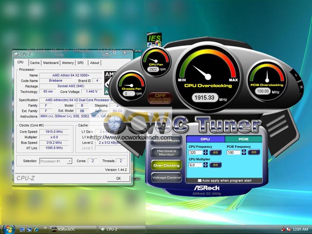
ASRock K10N750SLI-WiFi is the first board we review that is based on the nForce 750a SLI chipset. Based on the MCP72 series, this chipset is merely a castrated GF8200 with support of 2 PCIe x8 lanes for SLI Support and Hybrid SLI. Features wise, this board has almost all the necessary that you could thnik of. 6 x Serial ATAII 3.0 Gb/s connectors, support RAID (RAID 0, 1, RAID 0+1, RAID 5, JBOD), NCQ, AHCI and Hot Plug functions, - 1 x eSATAII 3.0 Gb/s connector, Gigabit LAN 10/100/1000 Mb/s, 2 x IEEE 1394 headers (one port on back panel, one header on board). In addition, it has a 7.1 CH Windows® Vista™ Premium Level HD Audio with Content Protection, supports DAC with 110dB dynamic range (ALC890 Audio Codec), DTS (Digital Theater Systems). There is also 1 x WiFi/E header. The backplate also has 1 x Coaxial SPDIF Out Port, 1 x Optical SPDIF Out Port, 1 x eSATAII port, 1 x RJ-45 LAN Port with LED, 1 x IEEE 1394 port, 6 x USB 2.0 Ports. ASRock also included IES (Intelligent Energy Saver) to help you save the world. It is said to effectively increase Voltage Regulator Efficiency by 16% and decrease its Voltage Regulator power consumption by 48% without reducing CPU performance and reliability. Performance wise, this board runs pretty well similar to most of the nForce chipsets with external graphics card. We have seen that both SLI and Hybrid SLI does give the performance a boost in the benchmarks. In terms of overclocking, this board has a lot of options for you to tweak. If you have only looked at the BIOS screen shots, you will be shocked that it is actually a ASRock BIOS. The options are plenty and the voltage ranges are high too. See Gallery for more. If you pair it up with a X2, it is the old familiar BIOS. If you use a Phenom, you are presented with a somewhat confusing option. There are two options, a CPU Freq Multiplier and a divider. I am still pondering why they make it so confusing with two options controlling the multiplier. In our test with a X2 5000+, we managed to push the HTT to a max of only 320MHz x 6 using OC Tuner. Voltages used : CPU =1.4v, Vdimm=2.1v. Anything beyond that results in no BOOT or Blue screen. As for maximum o/c the CPU multiplier can be raised to 16x200=3.2GHz on the BE X2 5000+.
In conclusion, this board amazed me. It is very complete as a all round solution. The down side would be the temperature of the chipset. Perhaps an active heatsink could be used to replace it. Although Phenom supports DDR2-1066, this board only supports DDR2-800. This is probably a chipset limitation. The SLI peddle switch is also kind of old school. With more SLI graphics cards using up two slots, perhaps it could be a better idea not to put the two slots too close to each other.
Pros
Cons
Ratings Here are my ratings out of 10.
|
|
(C) Copyright 1998-2008 OCWorkbench.com
|